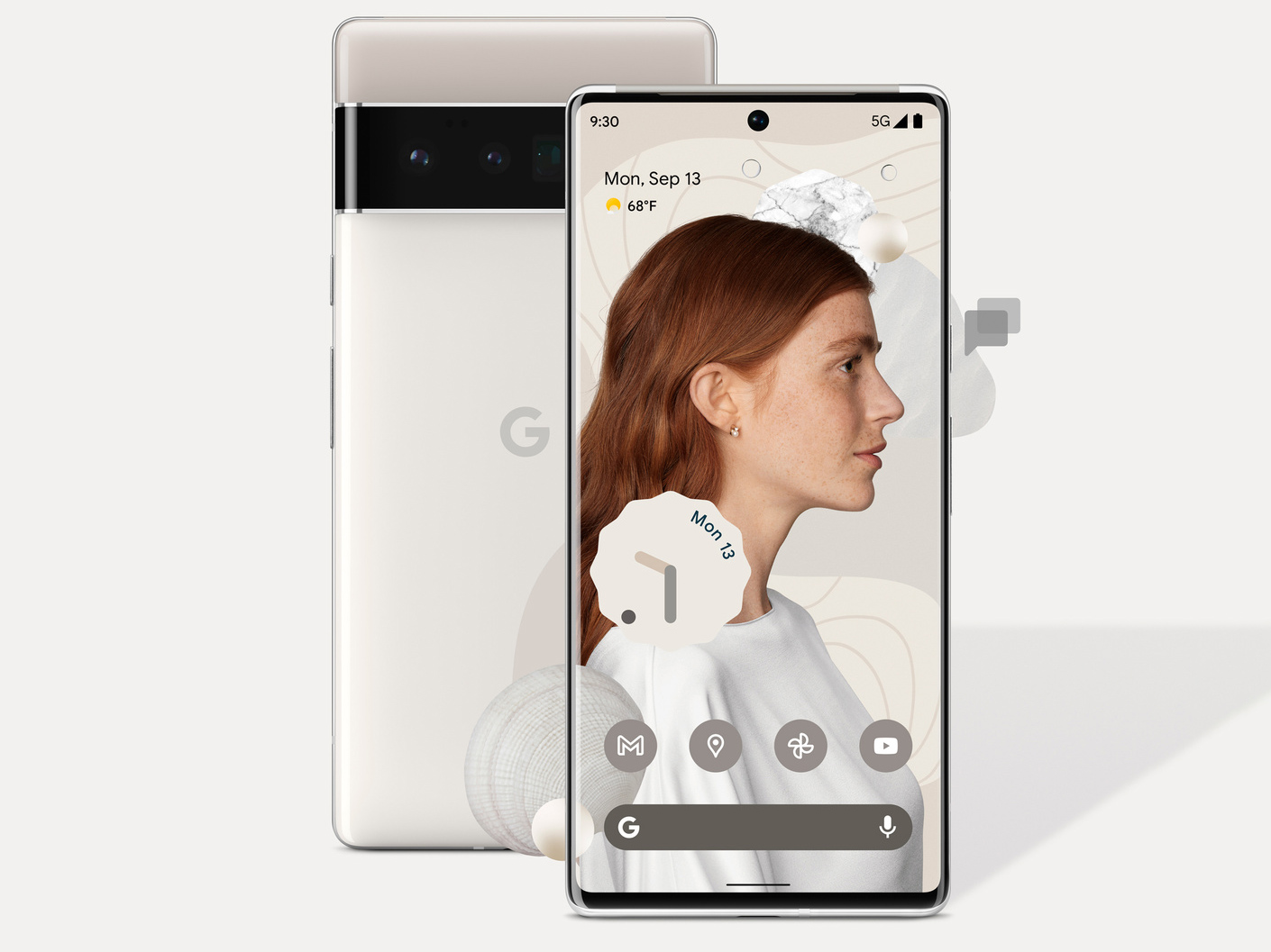
The Pixel 6 is official, with a wild new camera design, incredible pricing, and the new Android 12 OS. The headline component of the device has to be the Google Tensor "system on chip" (SoC), however. This is Google's first main SoC in a smartphone, and the chip has a unique CPU core configuration and a strong focus on AI capabilities.
Since when is Google a chip manufacturer, though? What are the goals of Tensor SoC? Why was it designed in its unique way? To get some answers, we sat down with members of the "Google Silicon" team—a name I don't think we've heard before.
Google Silicon is a group responsible for mobile chips from Google. That means the team designed previous Titan M security chips in the Pixel 3 and up, along with the Pixel Visual Core in the Pixel 2 and 3. The group has been working on main SoC development for three or four years, but it remains separate from the Cloud team's silicon work on things like YouTube transcoding chips and Cloud TPUs.
Phil Carmack is the vice president and general manager of Google Silicon, and Monika Gupta is the senior director on the team. Both were nice enough to tell us a bit more about Google's secretive chip.Most mobile SoC vendors license their chip architecture from ARM, which also offers some (optional) guidelines on how to design a chip using its cores. And, apart from Apple, most of these custom designs stick pretty closely to these guidelines. This year, the most common design is a chip with one big ARM Cortex-X1 core, three medium A78 cores, and four slower, lower-power A55 cores for background processing.
Now wrap your mind around what Google is doing with the Google Tensor: the chip still has four A55s for the small cores, but it has two Arm Cortex-X1 CPUs at 2.8 GHz to handle foreground processing duties.
For "medium" cores, we get two 2.25 GHz A76 CPUs. (That's A76, not the A78 everyone else is using—these A76s are the "big" CPU cores from last year.) When Arm introduced the A78 design, it said that the core—on a 5nm process—offered 20 percent more sustained performance in the same thermal envelope compared to the 7nm A76. Google is now using the A76 design but on a 5nm chip, so, going by ARM's description, Google's A76 should put out less heat than an A78 chip. Google is basically spending more thermal budget on having two big cores and less on the medium cores.
So the first question for the Google Silicon team is: what's up with this core layout?
Carmack's explanation is that the dual-X1 architecture is a play for efficiency at "medium" workloads. "We focused a lot of our design effort on how the workload is allocated, how the energy is distributed across the chip, and how the processors come into play at various points in time," Carmack said. "When a heavy workload comes in, Android tends to hit it hard, and that's how we get responsiveness."
This is referring to the "rush to sleep" behavior most mobile chipsets exhibit, where something like loading a webpage has everything thrown at it so the task can be done quickly and the device can return to a lower-power state quickly.
"When it's a steady-state problem where, say, the CPU has a lighter load but it's still modestly significant, you'll have the dual X1s running, and at that performance level, that will be the most efficient," Carmack said.
He gave a camera view as an example of a "medium" workload, saying that you "open up your camera and you have a live view and a lot of really interesting things are happening all at once. You've got imaging calculations. You've got rendering calculations. You've got ML [machine learning] calculations, because maybe Lens is on detecting images or whatever. During situations like that, you have a lot of computation, but it's heterogeneous."
A quick aside: "heterogeneous" here means using more bits of the SoC for compute than just the CPU, so in the case of Lens, that means CPU, GPU, ISP (the camera co-processor), and Google's ML co-processor.
Carmack continued, "You might use the two X1s dialed down in frequency so they're ultra-efficient, but they're still at a workload that's pretty heavy. A workload that you normally would have done with dual A76s, maxed out, is now barely tapping the gas with dual X1s."
The camera is a great case study, since previous Pixel phones have failed at exactly this kind of task. The Pixel 5 and 5a both regularly overheat after three minutes of 4K recording. I'm not allowed to talk too much about this right now, but I did record a 20 minute, 4K, 60 FPS video on a Pixel 6 with no overheating issues. (I got bored after 20 minutes.)
So, is Google pushing back on the idea that one big core is a good design? The idea of using one big core has only recently popped up in Arm chips, after all. We used to have four "big" cores and four "little" cores without any of this super-sized, single-core "prime" stuff.
"It all comes down to what you're trying to accomplish," Carmack said. "I'll tell you where one big core versus two wins: when your goal is to win a single-threaded benchmark. You throw as many gates as possible at the one big core to win a single-threaded benchmark... If you want responsiveness, the quickest way to get that, and the most efficient way to get high-performance, is probably two big cores."
Carmack warned that this "could evolve depending on how efficiency is mapped from one generation to the next," but for the X1, Google claims that this design is better.
"The single-core performance is 80 percent faster than our previous generation; the GPU performance is 370 percent faster than our previous generation. I say that because people are going to ask that question, but to me, that's not really the story," Carmack explained. "I think the one thing you can take away from this part of the story is that although we're a brand-new entry into the SoC space, we know how to make high-frequency, high-performance circuits that are dense, fast, and capable... Our implementation is rock solid in terms of frequencies, in terms of frequency per watt, all of that stuff. That's not a reason to build an all-new Tensor SoC."
reader comments
87